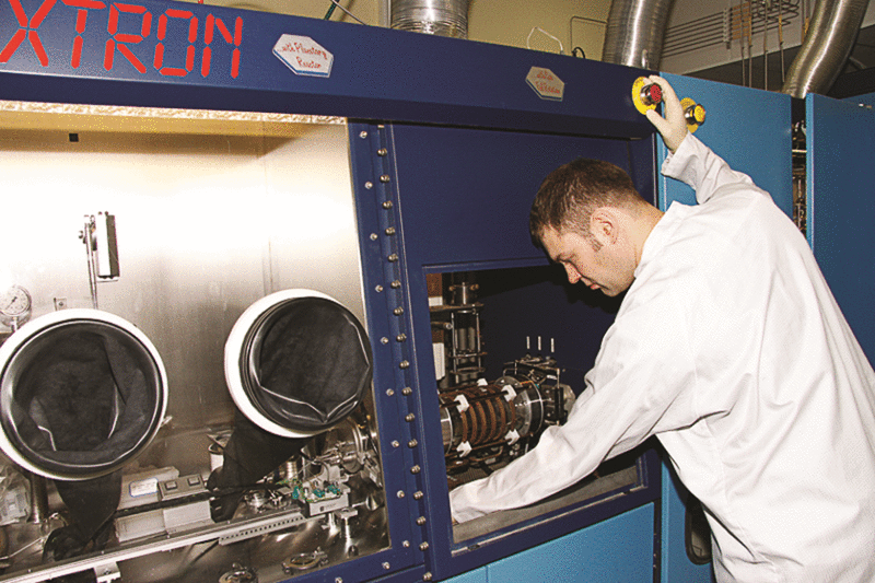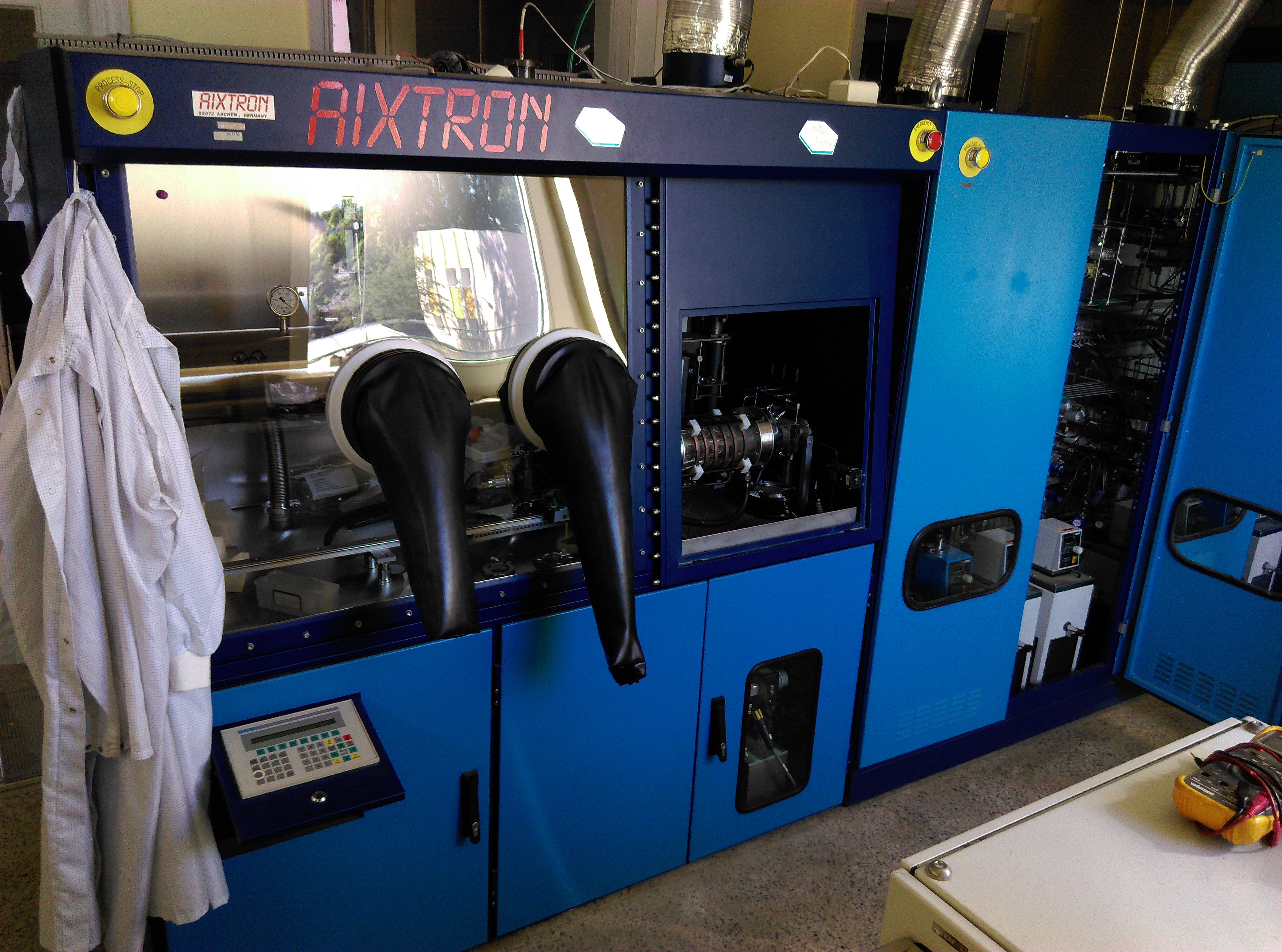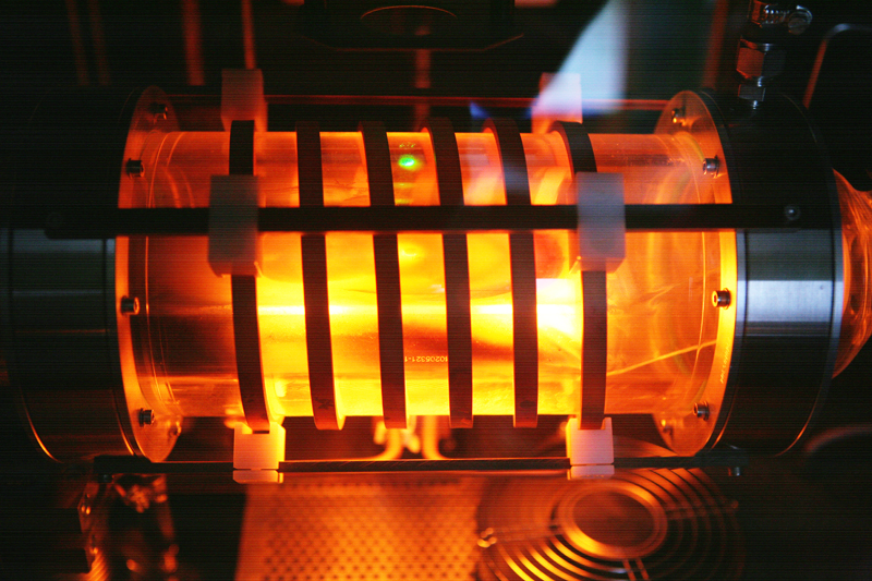

  MOCVD MOCVD technique is a major process used in semiconductor industry and electronic device fabrication due to the possibility to grow epitaxial monocrystalline thin films in a large scale, due to the variety of available materials and compounds, and due to the well controllable deposition process. Semi-industrial MOCVD has been utilized at ISSP for research of III-Nitride epitaxial heterostructure growth including LED structures. Uniform MOCVD growth of β-Ga2O3 thin film has been previously demonstrated, and single crystallinity was achieved for Ga2O3 thin films and Ga2O3/AlGaO heterostructures. ISSP will soon install materials system, enabling state-of-the-art growth capabilities in the ultra-wide bandgap range. The system will allow ISSP researchers to develop oxide semiconductor materials, namely gallium oxide (Ga2O3, Al2O3, Ir2Ox), integral to promising ultra-wide bandgap semiconductors for UV-optoelectronic and power electronic device applications. The system will enable the growth of (Al, Ga, Ir)2O3, which will provide a materials platform for researchers to investigate the fundamental physical properties of this emerging material and maximize the benefits provided by the system - critical to advanced device designs and its broad application in society. The renovated gallium oxide-capable MOCVD is a radio frequency-heated quartz tube system specially designed for gallium oxide and aluminium gallium oxide epitaxy. The new system design, capable of depositing on 50 mm substrates at temperatures as high as 1200°C.
|

|

Fax: (+371) 67132778 Phone: (+371) 67251691 |


|

|